Entering the quantum age
Welcome to the nanoworld—and to the realm of quantum physics, where standard rules of reality no longer apply. Nanoparticles and nanomaterials have properties that open up completely new possibilities: building ultra-fast quantum computers to name just one. Project leader Roman Fasel and the CarboQuant team at the Swiss Federal Laboratories for Materials Science and Technology (Empa) want to exploit these properties to develop nanomaterials that can transform quantum technology into an everyday technology.
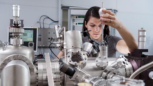
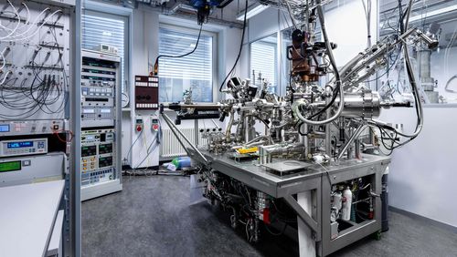
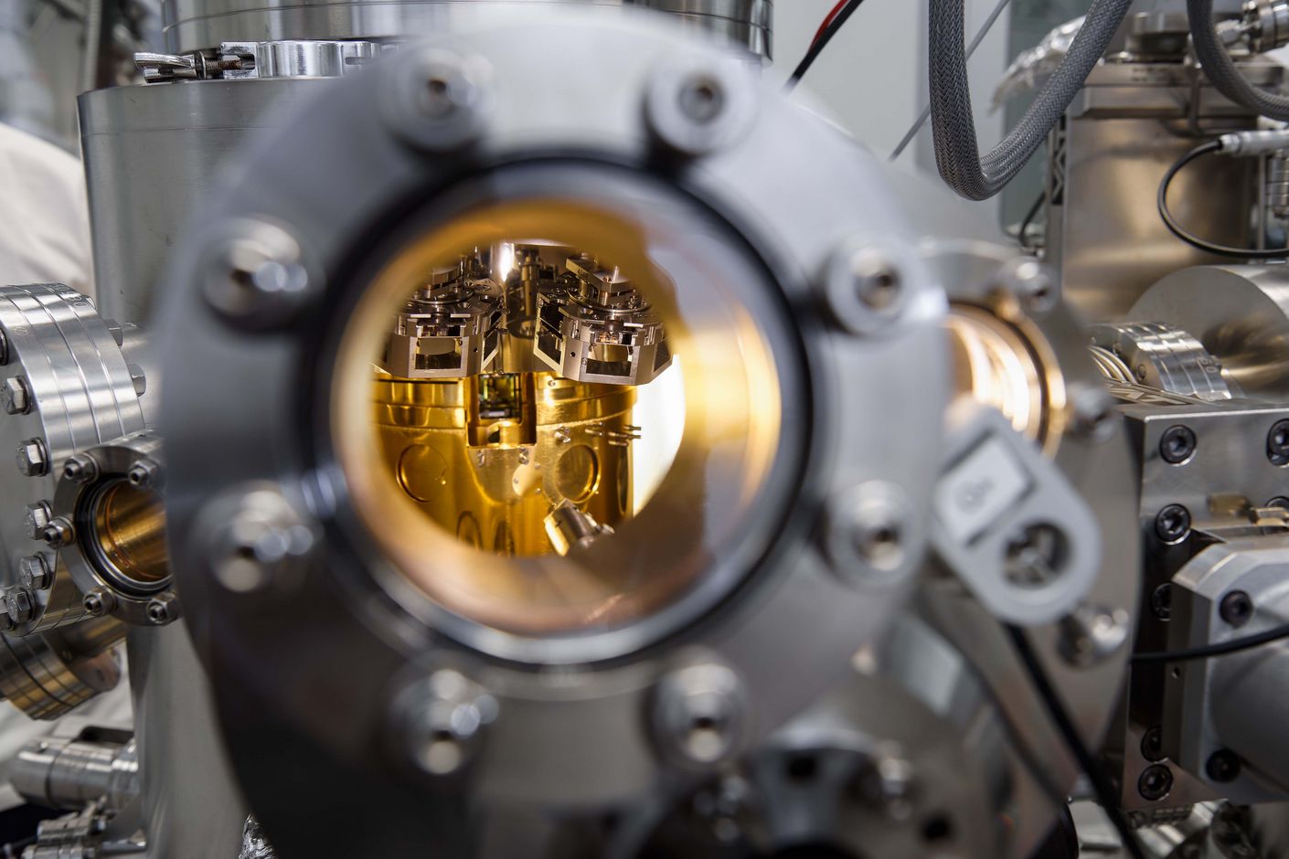
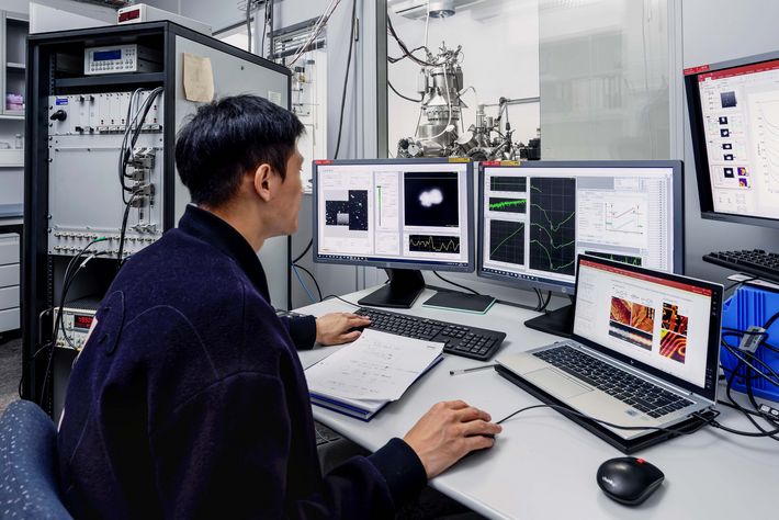
A large, strange-looking contraption made of shining metal stands in the middle of the room: a scanning tunnelling microscope. Where the various “peepholes” are located is not immediately obvious—they are hidden away in the tangle of pipes, hoses, screws, plates and cables. But not to worry: Gabriela Borin Barin, chemist and materials engineer in the CarboQuant team at Empa’s nanotech@surfaces Laboratory, knows the complex machine inside and out. Walking towards one of the circular windows, she peers into the scanning tunnelling microscope and turns a knob to move a delicate pair of pliers positioned within, where the interior environment is an almost perfect vacuum. With the knob, Borin Barin continues to manoeuvre the pliers very carefully deeper into the device in order to remove a material sample from a minuscule shelf.
The material that Borin Barin is about to measure is brand new. She triggered a series of chemical reactions on a gold foil to fabricate a specific carbon structure: a long thin ribbon consisting of a single layer of interconnected atoms—a nanostructure. Borin Barin first designed the nanostructure and then synthesised it on the basis of her concept. It is precisely these kinds of carbon nanoribbons that she and her CarboQuant colleagues at Empa, in Dübendorf, Switzerland, are planning to use to create completely novel electronic components. Specifically, they want to develop electronic components based on quantum states in order to build computers so powerful that the supercomputers of today will look like humble pocket calculators in comparison.
Infinitesimal dimensions
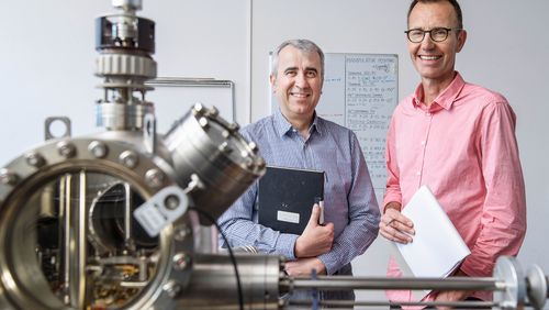
To illustrate the point, Oliver Gröning, deputy head of the CarboQuant team, rummages in his pocket for his smartphone. “The phone looks modern, but the technology inside is fifty years old,” Gröning says. Of course, the processors in today’s electronic devices are faster and smaller than ever before, “but the physics they’re based on hasn’t changed”.
Researchers in the CarboQuant project have now set their sights on the next big development. Or rather, on a smaller dimension: the nanodimension. Indeed, when we step into the nanoworld, classical physics enters the realm of quantum physics. “Quantum physics starts at a size of about ten nanometres,” Gröning explains. One nanometre is equal to one thousand-millionth of a metre. For comparison, a single human hair measures seventy thousand nanometres in circumference.
New rules apply
And in the nanoworld, the rules of our visible reality no longer apply—in quantum physics, particles can simultaneously have physical properties that contradict each other in classical physics. Or two particles can be physically far apart yet nonetheless linked and capable of influencing each other. “It’s these types of quantum effects that we aim to exploit,” Gröning says. To do so, the researchers must be able to control their materials down to the nanodimension—meaning down to the atom.

(Photo: Empa, Dübendorf)
Distinguishing individual atoms
In the lab, Gabriela Borin Barin continues to turn the knob carefully, moving the pliers with the sample and placing it into the section of the scanning tunnelling microscope where the material will be measured. Only the gold foil on which the nanostructures were synthesised can be seen—the new material itself is invisible to the naked eye.
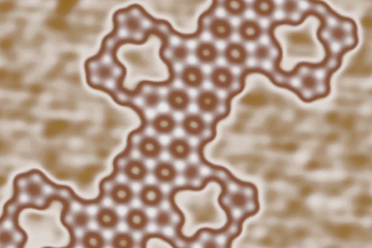
The entire procedure is extremely sensitive. “The scanning tunnelling microscope reacts to each and every vibration,” Borin Barin says. For this reason, the device is housed in the lower level of the lab building, where there is less risk of disturbance. In addition, the microscope is placed on a type of shelf equipped with a system capable of absorbing even the slightest of vibrations. These precautions ensure that the microscope’s measurements can be rendered as such high-resolution images that the researchers are able to identify individual atoms in their newly created materials.
Every shape a new material
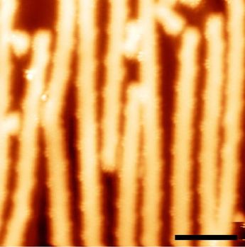
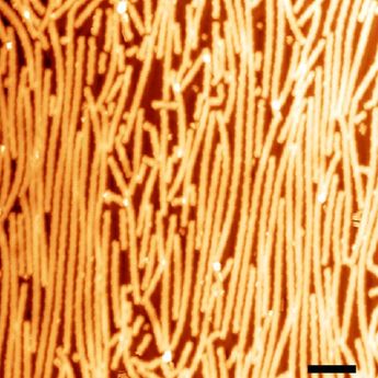
The shape of the nanoribbons is not left to chance. The long edges hold all the potential—indeed, the structure of these edges is what determines the material’s quantum electronic properties. And although the nanoribbons designed and synthesised by the team only differ at the edges, they have fundamentally different electronic properties. “By slightly tweaking the shape of the nanoribbons, we’re creating an entirely new material,” says Gröning.
But to what end? To answer this question, a comparison with conventional, bit-based electronics is useful. Bits, the smallest computational unit, can have either one of two states: they can be a zero or a one. In the quantum world, however, these two states can overlap: it is possible for a unit to be a zero, a one—or both states simultaneously. This property is what enables circuits made of qubits—the components in quantum computers—to perform several computational operations at the same time, whereas a standard, bit-based circuit functions on a linear timeline. This means that the performance of a quantum computer increases exponentially with each additional qubit.
Another quantum effect is the linking of particles, called quantum entanglement in technical jargon. Quantum entanglement is used to program quantum computers or to write code for extremely secure encryption.
Exploiting quantum effects
The Empa researchers want to furnish their CarboQuant nanoribbons with these kinds of useful quantum effects and are particularly interested in electron spin: the rotational momentum of electrons. The team have already discovered that, with the right nanoribbon structure, the electron spins of both edges can be linked. In turn, this creates a kind of superhighway for spin states, comparable with the electric charge pathways in conventional electronics. “If we succeed in controlling these spin states, we can use them for quantum electronic components,” Gröning says.
Synthesis in a vacuum
Back in the lab, Borin Barin begins to take measurements of her nanoribbon sample. Because the procedure is so delicate, measuring the material takes place in a high vacuum chamber, where a barely visible, ultra-fine needle made of a platinum-iridium alloy probes the sample, causing electrons to flow across the minuscule distance between the tip of the needle and the sample. This generates a measurable electric current, and the effect—known as quantum tunnelling—makes it possible to map a precise image of the new nanoribbon down to the last atom. Now, Borin Barin has to wait just a few hours until the image of her nanoribbon is ready.
Nanoribbons are not only measured but also synthesised in a vacuum. To be precise: in a synthesis chamber separate from the microscope chamber. Borin Barin transfers the starting materials (the gold foil and the precursor molecules that will be synthesised to form a nanoribbon) through a type of ventilation shaft into the ultra-high vacuum. When moving the materials into the synthesis chamber, the shaft is opened and then quickly reverted to a vacuum state. “If we had to open the synthesis chamber itself, we would have to wait an entire week for the system to be ready for use again,” Borin Barin explains.
The synthesis procedure itself consists of a sequence of various cooling and heating phases, up to a maximum temperature of four hundred degrees Celsius. If the researchers want to fabricate a specific new structure, they must first go through a step-by-step discovery process to identify the necessary conditions. The scanning tunnelling microscope is also used to monitor whether the intended reactions actually take place and whether the nanoribbon structure produced corresponds to their designs.
The key to success
Another, smaller device that looks like a distant cousin of a diving bell is located in a corner of the lab. This machine is responsible for automatically carrying out the synthesis processes. The nanoribbons it synthesises can be transferred into a normal environment (ambient atmosphere), enabling the researchers to analyse the materials’ optical and electronic properties outside the vacuum chamber and to integrate them into electronic components.
The researchers have been working for quite some time on developing the high-precision synthesis methods for their nanoribbons. Three years ago, they began to understand how they would have to design the nanostructures to create stable spin quantum effects. “That’s the key to future developments,” says Gröning. “We’ve now reached the point where we can permanently encode complex quantum states in the nanostructures. Now the next great challenge is understanding how to control and further develop these quantum states.” Thanks to funding from the Werner Siemens Foundation, the team will be able to spend the next few years converting these challenges into ever more successes.
Text: Santina Russo
Photos: Felix Wey
