
The microchip of the future
From espresso machines to huge mainframe computers, microchips are in almost every electronic device we use. But now, the push to get even smaller has hit a wall: the smaller the components, the less efficient the chip—and too much energy is lost via leakage currents or heat loss. If current testing on the single-atom switch is successful, this problem could belong to the past.
“We’ll need even smaller and more efficient chips in future, meaning a fundamentally new technology is necessary,” says Professor Jürg Leuthold, head of the Institute of Electromagnetic Fields at ETH Zurich. Through his research, Leuthold aims to revolutionise the semiconductor industry, and to realise this ambitious goal, he has joined forces with Professor Thomas Schimmel from the Karlsruhe Institute of Technology and Professor Mathieu Luisier from ETH Zurich to lay the groundwork for the microchips of the future. The overarching goal? Chips that are 100 times smaller and 100 times more energy efficient—while at least retaining the current speed of data processing.


Dancing atoms
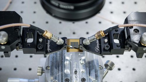
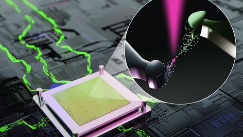
The researchers have developed a component for microchips that’s just 10 nanometres long. But the fundamental innovation is less its size than that it functions at the atomic level. The nano-component is made of silver and platinum pads that approach one another until only a tiny gap remains. Using minimal electrical voltage, a single atom is then slipped between the two pads, causing a digital signal to be emitted (cf. image). This principle is what gave rise to the name “atomic-scale technology”.
In the computers of tomorrow, millions of single atoms will be performing this dance to transmit signals. The basic principle is reminiscent of the human brain, with its fireworks of neurotransmitters and ions that shoot back and forth between billions of nerve cells. “The human brain requires very little energy to achieve its enormous processing power. We want to create comparably efficient structures with atomic-scale technologies,” Leuthold explains.
Amazing possibilities
The new nano-component being developed in Zurich and Karlruhe is a veritable powerhouse. It can switch processes on and off, and is therefore suitable for use in all electronically steered devices. At the same time, it also processes and stores data. “It’s the smallest possible storage unit imaginable. As such, we’re navigating the borders of physics.”
But the developments aren’t limited to new frontiers. The tiny chip is also a modulator that can transform electrical signals into light signals and vice-versa—an extremely useful feature for transmitting data in fibre optic cables. For instance, when sending signals from a cell phone or a computer, the nano-components can be transformed into optical (photonic) signals, which are reverted to their original form when received. If the nano-components are shunted by the million, they could make a major contribution to dealing with the continually increasing flow and ever-faster transmission of data in the internet.
 on and off.")
Asia calling
The research alliance between Zurich and Karlsruhe is now united in the new Centre of Atomic Scale Technologies. Although the collaboration has only recently begun, the research groups involved were predestined for the task at hand. Thomas Schimmel is a pioneer of electronic circuits at the level of the atom, and Jürg Leuthold has demonstrated in his past research that photonic switches are possible at the atomic level. Moreover, Leuthold was the first researcher able to place both optical and electronic switching elements on the same chip.
As such, it comes as no surprise that major firms from the Asian semiconductor industry have expressed great interest in Jürg Leuthold’s research. But the Zurich professor has another aim in mind: “The next Silicon Valley should be in Europe. And now, thanks to the Werner Siemens-Foundation, we can take on a leading role in semiconductor electronics.”
To begin its work, the Centre of Atomic Scale Technologies is using initial Foundation funding to create 14 positions for PhD candidates and postdocs, and to purchase additional equipment to analyse and optimise nano-components.
Partnering with industry
By 2021, the researchers aim to have laid the theoretical and technological groundwork necessary to create a prototype processor with 20 single-atom components. By 2025, they plan to have complex processors ready for production. The ultimate goal is to integrate the new components into common silicon chips (CMOS chips), but the researchers also see potential for use in artificial intelligence, machine learning and autonomous systems.
To make the dream of a European Silicon Valley reality, the team will soon need strong partners from industry. To be sure, there should be plenty of interest: the project in Zurich and Karlsruhe holds great promise and has the potential to revolutionise microelectronics—and our everyday electronic devices.
Text: Adrian Ritter
Photos: Felix Wey
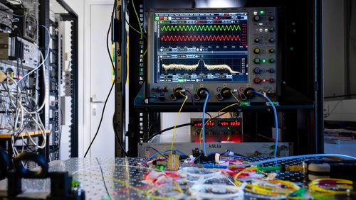
 watching an experiment at Jürg Leuthold’s Center for Single Atom Electronics and Photonics at ETH Zurich.")
![[Translate to English:]](/fileadmin/_processed_/5/3/csm_Report24-Nachhaltigkeit-Muster_2c7b6666b3.gif "[Translate to English:]")

.")


