und Andreas Bett wollen den vielversprechenden Tandemsolarzellen zum Durchbruch verhelfen.")
 und Andreas Bett wollen den vielversprechenden Tandemsolarzellen zum Durchbruch verhelfen.")
Ultra-efficient solar cells
Tandem solar cells are much more efficient than conventional silicon cells—but they’re also very expensive to manufacture. This is set to change thanks to a project recently awarded funding from the Werner Siemens Foundation: at the Fraunhofer Institute for Solar Energy Systems ISE in Freiburg im Breisgau, Germany, researchers are developing ultra-thin, highly efficient solar cells.
Photovoltaics systems are probably our best shot in combating global warming. After all, the sun delivers as much energy per hour as humans consume per annum—in theory, solar cells could easily supply the world with renewable energy. In reality, however, we would have to install an enormous number of solar modules to meet our ever-growing demand for energy. Forecasts predict that, as of 2037, solar modules with a 3.4-terawatt capacity will have to be built worldwide, and that every year.
“If constructed with today’s silicon technology, these PV systems would cover an area larger than a third of Switzerland on an annual basis,” says Frank Dimroth, head of the Department for III-V Photovoltaics and Concentrator Technology at the Fraunhofer Institute for Solar Energy Systems ISE (Fraunhofer ISE) in Freiburg, Germany. In addition to using up so much land, this scenario would also consume huge amounts of material and energy. Manufacturing 3.4-terawatt of solar modules per year on the basis of crystalline silicon consumes twice the amout of solar energy currently produced worldwide, as Dimroth explains, adding, “That’s why we need more efficient, resource-saving solar technologies.”
Developing innovative processes to produce tandem solar cells is the aim of the new “Sustainable energy transition through high-efficiency tandem photovoltaics” project. Frank Dimroth leads the innovative undertaking together with Andreas Bett, director of Fraunhofer ISE and professor at the Institute of Physics at the Albert Ludwig University of Freiburg. The Werner Siemens Foundation (WSS) is financing the research with a total of 14 million euros over the next 7.5 years; the Fraunhofer Society is contributing an additional 1.4 million euros.

More layers, greater output
The heart of the project is a technology called III-V multi-junction solar cells. This type of solar cell consists of several semiconductor layers made up of elements from the third and fifth groups of the periodic table—gallium, indium, arsenic and phosphorus, for example. Because each layer absorbs a different spectrum of sunlight, “tandem” solar cells attain excellent conversion efficiency. Indeed, compared to current state-of-the-art silicon-based cells, the same surface area can produce roughly a third more output.
Although multi-junction solar cells have been used in space for some twenty years to power satellites, their use here on Earth is uncommon. The main problem is that material and production costs are about one hundred times higher than for standard silicon-based solar cells. This is because the materials needed to build the tandem cells are both much less common and more expensive than silicon, Frank Dimroth explains. “In addition, todays manufacturing processes are complex and they were developed for the production of small batches in a premium market segment.”
In their endeavour to make the manufacture of III-V multi-junction solar cells marketable, the researchers in the new WSS project plan to develop ultra-thin solar cells that use minimal amounts of material. Currently, a silicon solar cell is about one hundred and forty micrometres thick. The future III-V semiconductors from Freiburg will measure a mere three micrometres—or less than a tenth of a human hair. What’s more, the development is expected to significantly lower manufacturing costs across all production phases. However, to understand how the researchers plan to proceed, it’s first necessary to grasp how a III-V multi-junction solar cell is created.
Fracture line inside the substrate
The production of III-V multi-junction solar cells can be divided into three main steps, the first of which is fabricating a growth substrate—called a “wafer”. For this, a single-crystal cylinder of high-purity germanium is grown and subsequently cut into thin slices.
In the second step, several layers of III-V semiconductors—gallium arsenide or gallium indium phosphide, for example—are deposited onto the germanium substrate. The metal elements are fed into the epitaxy reactor using metalorganic or hydride gases which decompose at high temperatures and release their metal atoms. When the conditions are right, these atoms arrange themselves on the germanium lattice to form a perfect crystal lattice. This ordered growth is also known as epitaxy. To fabricate a solar cell from these layers, several processes are required in the third and final step: applying nano-mirror coatings, for example, evaporating contacts and protecting edges.
The researchers are aiming to innovate and optimise processes in all three phases. In step one, their main goal is reducing resource consumption by the reuse of growth substrates. Today, the wafer is generally left in the finished solar cell. “But we want to detach these ultra-thin semiconductor layers from the substrate,” Frank Dimroth explains—because the valuable materials can be reused up to a hundred times. For this, the researchers are devising a clever strategy drawing on electrochemical methods: just a few hundred nanometres below the surface of the germanium wafer, they create a porous layer that functions as a predetermined breaking point—a fracture line, so to speak—for separating the semiconductor layers from the substrate. Dimroth adds a caveat: “We still need to conduct a great deal of in-depth research to perfect this technology.”


Speed and automation
A key development in the second step is high-throughput epitaxy. The equipment currently used to grow crystals for III-V multi-junction solar cells is relatively slow and has a low throughput. Over the past three years, researchers at Fraunhofer ISE have developed a new, much more powerful epitaxy machine. “Our aim is to reduce a process that currently takes two hours to just ten minutes,” Dimroth says. They expect to have the prototype delivered to Freiburg in the first half of 2025; the first tests are scheduled for autumn.
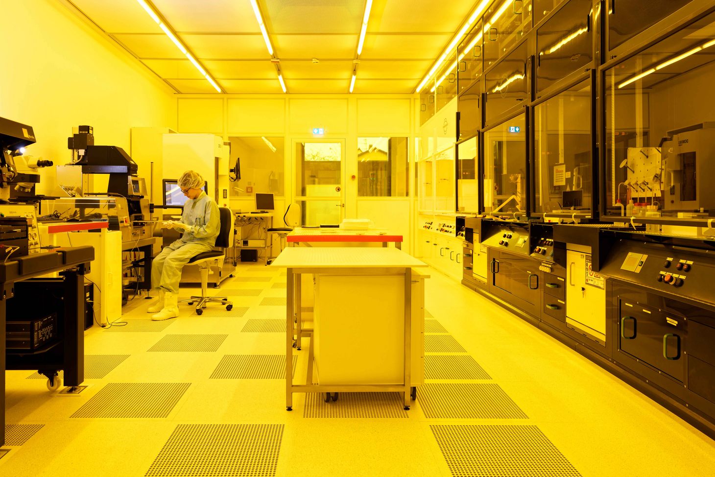
The researchers are also re-imagining production processes in the third step. Currently, III-V multi-junction solar cells are fabricated in clean rooms using microelectronics technology such as photolithography, chemical etching and vapour deposition—all of which go back to the semiconductor industry. And all of which have several drawbacks: they require a lot of man- and electric power, they’re expensive, have a low throughput and use toxic photoresist materials. “Our aim is to create an economical alternative that can be scaled up to producing square kilometres of solar cells per year,” Frank Dimroth says.
The researchers won’t have to reinvent the wheel for these innovations, as many underlying processes are already used in the manufacture of silicon-based photovoltaics. Dimroth explains that a combination of printing, laser and spraying processes in addition to electroplating will help simplify and automate production: “Our concept envisions that the wafer-thin cells will move through a machine on a conveyor belt and come out fully processed at the end.” Fraunhofer ISE offers particularly good conditions for these production lines, as staff there have a great deal of expertise in silicon photovoltaics.
Despite the good overall starting situation, however, the researchers face numerous challenges. For example, multi-junction solar cells and silicon cells have different structures, so production processes can’t be copied one-to-one. In addition, today’s semiconductor technologies are unmatched in terms of quality. “If we galvanise a metal onto the semiconductor instead of vapour-depositing it, the contacts between the two surfaces are compromised,” Dimroth explains. “We have to seek and find the right trade-off between quality and economical, large-scale production.”
Concentrated sunlight
In addition to classic tandem solar cells, the researchers are pursuing another highly promising technology: a combination of III-V semiconductor multi-junction solar cells with concentrator photovoltaics (CPV). In this process, low-cost lenses are used to amplify sunlight by a factor of one thousand before a tiny solar cell converts it into electricity. “This method uses one 1000 times less semiconductor material,” Frank Dimroth says.
A few years ago, the team produced a CPV solar cell that attains an efficiency of 47.6 percent when exposed to sunlight concentrated 665 times—a world record. Such concentrator photovoltaics systems work well in African countries and Australia where there is intense direct solar radiation. Here the technology could enable the production of renewable fuels like hydrogen or other energy carriers that are easy to transport and store.
Existing concentrator modules use III-V semiconductor multi-junction solar cells with their germanium substrate. “That’s why the cells—even with their small surface area—account for nearly half the total cost of a module,” Dimroth explains. “The cells we’re developing have the potential to lower production costs by a factor of ten.” If the Fraunhofer ISE researchers succeed in integrating the super-thin semiconductors into the concentrator modules, they calculate that sun-rich countries will be able to produce solar power for less than two euro cents per kilowatt hour.
Europe’s big chance
The ultra-thin cells are the centrepiece of the project—and probably also the biggest challenge. In addition to detaching the semiconducting materials from the substrate during production, the further processing steps bring their own set of difficulties. “It’s important that we keep the delicate layers stable at all times and that we ensure they don’t break,” Frank Dimroth says, adding that the second big challenge is to align all the many different processes so that manufacturing the novel solar cells becomes cost competitive—while nonetheless retaining the technology’s advantages. “We want to ensure the cells don’t lose efficiency during production,” he explains. “Our objective is the cost-effective fabrication of solar cells that have a conversion efficiency of thirty-five percent.”
If the ISE researchers meet with success, their development would give photovoltaics systems a major boost—the project could even serve as the starting point for reinvigorating Europe’s solar industry. For one, the innovative solar cells have such low demands in terms of energy and material that production in Europe is entirely feasible. “For another,” Dimroth says, “our technology is too complex for imitators to reconstruct.”
Facts and figures
Funding from the Werner Siemens Foundation
14 million euros
Project duration
2025 to 2032
Project leaders
Dr Frank Dimroth, Head of the Department for III-V Photovoltaics and Concentrator Technology, Fraunhofer Institute for Solar Energy Systems ISE Freiburg i. Br.
Prof. Dr Andreas Bett, Institute of Physics, Albert Ludwig University of Freiburg, Director of the Fraunhofer Institute for Solar Energy Systems ISE Freiburg i. Br.