
Ultra-thin and highly efficient
The conversion efficiency of multi-junction solar cells is much higher than that of the silicon-based cells commonly used in PV systems. Despite the technical edge, however, innovations at almost every stage of production are needed to make them economically competitive. Researchers in a new WSS project at the Fraunhofer Institute for Solar Energy Systems (Fraunhofer ISE) in Freiburg im Breisgau, Germany, have come up with some bold ideas.
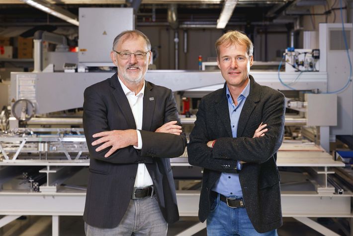
The Fraunhofer ISE campus in Freiburg im Breisgau can be best described as “sprawling”. And exactly how complex it is to produce a solar cell becomes clear as Frank Dimroth guides his visitor from building to building and innovation to innovation. Of course, the cells constructed here are no ordinary solar cells—they’re an entirely new invention. And they represent an innovation that could give Europe a second chance at becoming a leader in the global solar industry.
Frank Dimroth is head of the Department for III-V Photovoltaics and Concentrator Technology at Fraunhofer ISE. Together with ISE director Andreas Bett, he leads the new “Sustainable energy transition through high-efficiency tandem photovoltaics” project that the Werner Siemens Foundation is funding with a total of 14 million euros over the next 7.5 years. The Fraunhofer Society is contributing an additional 1.4 million euros to the research endeavour.
The centrepiece of the project is a technology called III-V multi-junction solar cells. This type of solar cell consists of two to six solar cells grown on top of each other, each of which is made up of elements from the third and fifth groups of the periodic table—gallium, indium, arsenic and phosphorus, for example. Because each cell layer absorbs a different spectrum of sunlight, these “tandem” solar cells attain excellent conversion efficiency of up to 47.6 percent. Compared to current state-of-the-art silicon PV modules, the same surface area of a tandem module can produce roughly a third more output.
Streamlining production, saving costs
This difference is in no way trivial, and the use of tandem cells would significantly reduce the amount of land and resources required for solar power plants. Despite their advantage in conversion efficiency, however, tandem solar cells have so far only become the standard choice in the space industry, where they supply satellites with electricity. “Our base materials are rarer and more expensive than silicon,” Frank Dimroth explains, adding that manufacturing processes also remain costly because it has never been a priority to develop affordable machines and processes for a mass market when only small quantities are needed for the niche space industry. “However, that’s what’s necessary if we’re to use the more efficient tandem solar cells here on Earth.”
The production of III-V multi-junction solar cells can be divided into three main stages, the first of which is fabricating a growth substrate—a “wafer”. In the second step, layers of III-V semiconductors are grown on the substrate in a process known as epitaxy. In the third step—processing—the actual solar cell is fabricated, complete with contacts, anti-reflective coatings and separation processes.
“Each of the three steps contributes roughly a third to the total production cost, meaning we have to make improvements in all three stages,” Dimroth explains. And he doesn’t mean a few cosmetic improvements, but rather a thorough overhaul: each part of the process must become many times more efficient. “Our aim is to make the process one hundred times less expensive,” he says. This amount corresponds to how much more it costs to manufacture a III-V multi-junction solar cell than a standard silicon-based cell.
Fracture line in the substrate
The researchers are developing numerous innovative strategies to achieve this lofty aim. With regard to the first step of developing the growth substrate (the wafers), the main solution is to save on material. The wafers, which are approximately 0.3 millimetres thick, provide a precise growth template for the III-V layers, which capture sunlight in the finished product. “We use an expensive element, germanium, on which we grow our solar cells,” Frank Dimroth says. “That’s why we want to detach the germanium substrate after the solar cell layers are deposited and reuse it several times.”
He demonstrates how this works in one of the labs in the ISE main building. Entering the space requires first putting on a protective lab coat and single-use shoe covers, as dirt particles and other impurities can compromise the experiments. Beneath a hood, a mount is used to affix a round wafer, which is then electro-chemically treated in a tank using hydrofluoric acid and two electrodes.
Dimroth says two key things happen in this process: “When we apply a negative voltage, it results in an extremely thin etching of the wafer’s surface.” And when a positive voltage is applied, the surface is passivated. Combining both steps with an additional thermal bake-out step makes it possible to create a porous layer a few hundred nanometres beneath the surface of the wafer.
This layer acts as a predetermined breaking point. “At the end of the manufacturing process, we can peel the semiconductor layers off the wafer and then reuse it several times,” Dimroth explains. Perfecting this technology will, however, require quite a bit of further research. “We’ve demonstrated that we can produce the layers. But the detachment process isn’t yet under control.” One of the first of many PhD theses to be written in the scope of the project began exploring this question in October 2025.
Unique epitaxy system
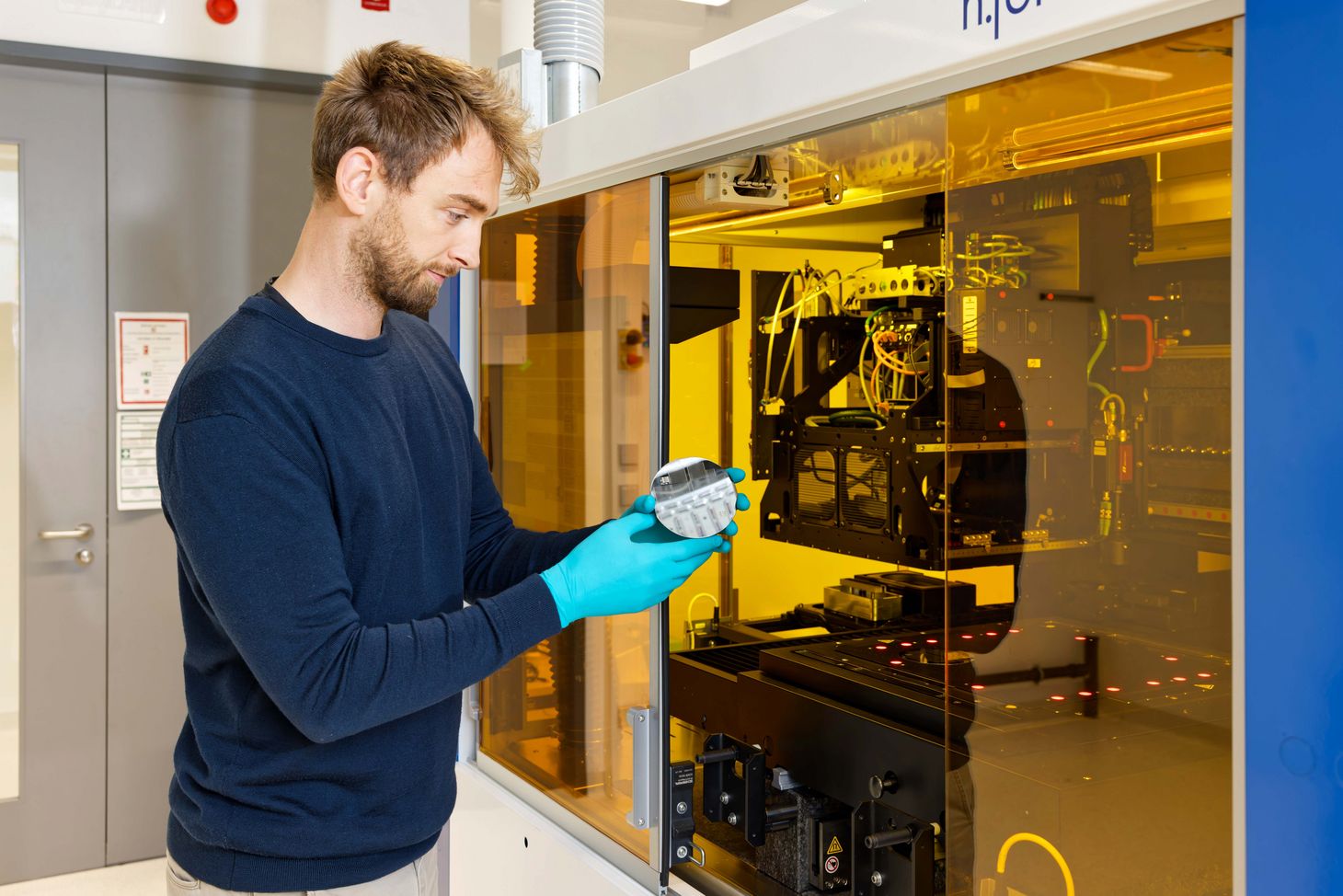
Before substrate detachment, however, the III-V semi-conductor layers of the solar cells’ must first be grown on the substrate. This process occurs incrementally in a complex machine that’s more than ten metres long. Frank Dimroth leads the way through corridors and stairways to the ISE epitaxy lab where, in addition to two existing tools, a third is now being set up. The new instrument promises to radically accelerate this second step in the development of solar cells.
The epitaxy machines currently used to grow crystals for III-V multi-junction solar cells are relatively slow and have a low throughput. Dimroth recalls that about four years ago, ISE specialists convened to discuss the design of an efficient machine: “We thought we’d have a plan for the processes within six months, which proved to be a bit too optimistic.”
Now, however, the system is ready: in collaboration with German medium-sized companies, the researchers have constructed a machine that meets the exact specifications for manufacturing III-V multi-junction photovoltaics. “Our aim is to reduce a process that takes two hours to one that requires just five minutes,” Dimroth says.
Grown layer by layer
During epitaxy, the germanium wafer is placed in the reactor chamber. Meanwhile, inside the epitaxy machine, the various semiconductor ingredients are mixed using a secret formula and enriched with dopants to produce the desired electrical conductivity. This mixture is then fed into the reactor chamber and distributed evenly over the wafers using a device that resembles a shower head. Inside the chamber, which has been heated to seven hundred degrees Celsius, the source molecules release their metal atoms—that then seek their place on the crystal lattice of the wafer. In the process, roughly twenty to forty semiconductor layers are deposited. The result is a solar cell structure that’s only a few micrometres thick—and nonetheless highly efficient.
The new epitaxy machine harbours even more innovations, one of which is simply the shape of the reaction chamber. Rather than being round, as in the older epitaxy system, it’s square-shaped, which enables more of the substrate’s surface to be covered. “This feature alone brings about twenty percent more efficiency,” Dimroth explains. Another major improvement is a novel technique for heating the reaction chamber to the required seven hundred degrees Celsius within a single minute. “The older machines needed twenty minutes to do the job,” Dimroth says.
A steel box is also fitted above the reaction chamber, which Dimroth says is a plasma generator the researchers use to ionise gases. The idea is that the plasma generator will facilitate breaking down the molecules, thus requiring less heat to aid the metal atoms in landing on the wafer. However, one potential problem is that the plasma might damage the semiconductors. Here, the project’s first PhD thesis in the area of epitaxy will examine whether the plasma generator is a net positive or negative for the process. “We’re entering new scientific ground,” is how Dimroth sums up the work.
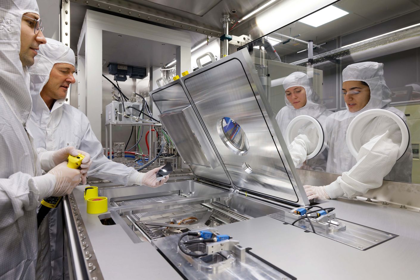
Clean room for lithography
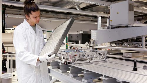
The third step in solar cell production—processing—takes place at the Center for High Efficiency Solar Cells, which Fraunhofer ISE opened four years ago. This is where the epitaxial wafers are processed into functional devices. Currently, this phase is conducted in clean rooms, which are costly and complex to operate. Often illuminated with yellow light, these spaces are used for work involving light-sensitive photoresists that create patterned areas (“masks”) on the light-facing side of the solar cell. Afterwards, ultra-thin metal layers are vapour-deposited onto this surface and the photoresist material is stripped away. What remains are fine, finger-like metal strips. “We want these metal contacts to cover as little of the cell area as possible so as not to interfere with its conversion efficiency,” Dimroth explains.
The projet’s first PhD thesis in this area is dedicated to studying how these production steps function when the tandem solar cell films are just a few micrometres thick—and to seeking potential solutions for lowering production costs. This especially includes replacing current microelectronic technologies with manufacturing techniques similar to those used for silicon photovoltaics.
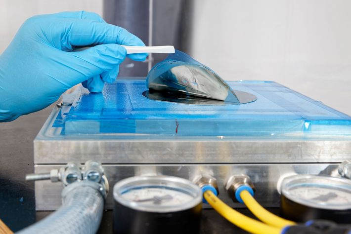
Printing of resists
Dimroth shows one such solution-in-progress in a lab room on the upper floor, where a large, two-by-two-metre inkjet printer is standing. The device can print structured resist layers on the solar cells with such precision that it would be possible to form metal contacts directly in the printed openings. This method has two advantages: it would be twenty times faster than current processes, and it would use less material for the coating. The drawback here is that the printer still requires some refinements: Dimroth says it can print to an accuracy of ten micrometres—but an accuracy of five micrometres is needed. “We’re working step-by-step to make the processes faster and more scalable—while retaining the necessary
precision.”
This is a critical point. In addition to competing with silicon-based solar cells in matters of cost, the novel solar cells must also retain their superior performance. “We want to ensure that production methods don’t cause the cells to lose efficiency,” Dimroth explains. “Our objective is a cost-effective fabrication of solar cells that have a conversion efficiency of thirty-five percent.” Should they succeed, nothing stands in the way of a new chapter in photovoltaics—one that even bears the label “made in Europe”.
 und Andreas Bett wollen den vielversprechenden Tandemsolarzellen zum Durchbruch verhelfen.")